Charge-Coupled devices (CCDs) |
|
We started to get to interested in the solid state properties of CCDs in
1996. Since then we investigated various properties of different front- and
back-illuminated scientific CCDs. Some examples like the characterization
of dark and bias frames, "ghosting", and the point spread function are described
in more details below. Introduction Dark Current Meyer Neldel rule Residual Images Point Spread Function Other Fields of Interest CCD Publications People In 1969 F. Sangster and K. Teer of the Philips Research Labs invented the Bucket-Brigade Device or BBD. This device basically transfers charge packets from one transistor to another. One year later, W. Boyle and G. Smith of the Bell Laboratories extended this concept by inventing a transport mechanism from one capacitor to another one. This new device got the name Charge Coupled Device or simply CCD. Initially designed as memory device, soon after the invention other applications were suggested. Since the CCD chip was sensitive to light it could be used as an image sensor. The first who recognized the potential of the CCD for high quality scientific images were astronomers. The CCD had a significantly higher sensitivity than the devices of that time: photographic film and vidicon tubes. With sensitivity 100 times greater than film, the CCD displaced other sensors within a few years. In the history of physics the invention of new or better equipment usually causes a cascade of other discoveries. The same was true after the invention of the CCD. Soon, previously invisible objects were discovered and increased our knowledge and understanding of the universe. Based on new data, theoretical models could be verified or were newly developed. The CCD chip is an array of Metal-Oxide-Semiconductor capacitors (MOS capacitors), each capacitor represents a pixel. By applying an external voltage to the top plates of the MOS structure, charges (electrons (e-) or holes (h+)) can be stored in the resulting potential well. These charges can be shifted from one pixel to another pixel by digital pulses applied to the top plates (gates). In this way the charges can be transferred row by row to a serial output register. The picture is the display of the electron distribution. Since electrons can be optical generated or more precisely excited from the valence in the conduction band, the CCD can be used as a light sensor for cameras. Cameras where the light penetrates through the gate structure to reach the region where electrons are collected, are called front-illuminated. More sophisticated in the production, but with a higher sensitivity are cameras where the CCD chip is exposed from the opposite side. These cameras are called back-illuminated. To insure charge transport from the back to the front side where the electrons are collected, the silicon bulk is thinned. The picture in a CCD is represented by the electron distribution on the CCD chip. But not all electrons give useful information of the pictured object. Electrons can be thermally excited into the conduction band. To minimize dark current scienctific CCDs are usually cooled. Images that include dark current can be corrected by subtracting a so call dark frame. A dark frame is a picture taken with a closed shutter. It contains the bias count as well as the count from thermally released electrons. The dark count is highly temperature and exposure time dependent. The energy necessary to excite electrons in the conduction band is called activation energy. Activation energies vary from pixel to pixel. Pixels with very low activation energies have higher count rates and are called “hot”. Some pixels show counts two or three times the average counts of the frame. The dark count typically doubles for every temperature increase of 5 to 10 Kelvin. For most pixels, the difference between dark counts and bias counts increases linearly over time. The temperature dependence of the dark current can be used to investigate the Meyer-Neldel rule (MNR). The MNR is an empirical law known since 1937. It states that the logarithm of the exponential prefactor is linearly related to the activation energy. Even though a number of theoretical models to explain the origin of the Meyer-Neldel rule are proposed, none of them is universally accepted. The dark count in a CCD gives a unique possibility (more than 222,000 samples can be used to verify the MNR) to investigate the MNR and its underlying mechanism. We found that the MNR arises naturally for a quantity where both an intrinsic process as well as a process involving impurities contribute. 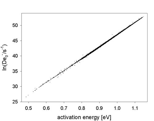
The logarithm of the exponential prefactor vs the apparent activation energy for all pixels on the CCD-chip. This plot contains more than 222,000 data points and clearly shows a behaviour according to the MNR. Impurities in the silicon crystal structure cause two different effects in CCD images. Impurity states between valence and conduction band make it easier for electrons to hop to the conduction band and cause an increase in the dark count signal. Another phenomenon caused by impurity states are lingering images. The pictures below show a dark frame taken shortly after an exposure with a laser beam. The counts for the laser picture were lower than the saturation counts for the CCD chip. The dark frames, which follow the picture, display residuals, the “ghost” of the previous picture, the lingering images. This effect has to be considered if the light intensity of the object is very low and a high resolution is required. During the exposure, photons excite electrons into impurity states located between the conduction and the valence band. In later exposures these electrons can be easily thermally excited into the conduction band. This can increase the number of dark counts especially for pixels with many loaded impurity traps. At low temperatures, trapped electrons can remain for hours or days in the impurity sites. Since the lifetime of these trapped electrons is highly temperature dependent an increase in temperature causes a release in a short period of time. Thus, ghosting can be minimized by heating up the chip before an exposure. 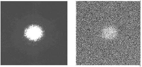
Left image: flat field of a laser spot; right image: dark image twenty seconds after the end of the flat field exposure. Note the "ghost" in the dark frame in the same part of the image where the image of the laser spot had been. Images taken with a Charge-Coupled Device (CCD) are the electron distribution over the chip, generated by incoming light. Electrons generated in a pixel area are not necessarily collected by the same pixel, but can diffuse into neighboring pixels because the electric field that collects the charge does not penetrate the entire chip. In these field-free regions, charge can diffuse randomly. Knowing the size of the field-free region helps to improve manufacturing and determine the modulation transfer function for a chip. We developed a technique for probing the diffusion of charge and to investigate the size of the field-free region. First, a source to obtain a light spot of less than one micrometer in diameter was created. Our idea was to take a glass fiber tip, similar to a Scanning Near Field Microscope (SNOM), which permits an easy change of wavelength. Different etch processes with hydrofluoric acid were used on a glass fiber to form a tip. After coating the tip with metal, a focused ion beam was used to cut the end giving an aperture size of less than one micron. We use a three-dimensional translation stage driven with a piezo to scan with a fiber tip over a single pixel. Different wavelengths, absorbed at different distances within the CCD, generate carriers at different distances from the pixel depletion region. The ability of carriers to diffuse will be less for wavelengths penetrating deeper, and thus a variety of wavelengths can be used to independently determine the field-free region. The response of a pixel was measured, depending on the location of the tip over the pixel. 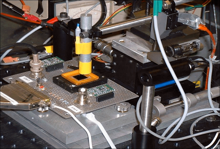
Experimental setup to measure the PSF of a CCD. IV characteristics of diodes CV characteristics of GaN devices in cooperation with NASA IR response of CCDs Ralf Widenhorn, Lars Mündermann, Armin Rest, and Erik Bodegom, "Meyer-Neldel
rule for dark current in charge-coupled devices," J. Appl. Phys.
89, 8179 (2001) pdf Ralf Widenhorn, D.A. Iordache, Erik Bodegom, “New Meyer-Neldel relations for the depletion and diffusion dark currents in some CCDs,” with , International Semiconductor Conference, 2004 Proceedings 2, 363 (2004) pdf Ralf Widenhorn, M. Fitzgibbons, Erik Bodegom, “The Meyer-Neldel rule for diodes in forward bias,” J. Appl. Phys. 96, 7379 (2004) pdf Matthias. Loch, Ralf Widenhorn, and Erik Bodegom, “Infrared response of charge-coupled devices,” Proc. of SPIE 5677, 201 (2005) pdf Ralf Widenhorn, D.A. Iordache, Erik Bodegom,“Interpreting fitting parameters of temperature dependence of dark currents in some CCDs,” International Semiconductor Conference, 2005 Proceedings 2, 327 (2005) pdf A.J.P. Theuwissen, M.F. Snoeij, X. Wang, P. R. Rao, E. Bodegom, “CMOS Image Sensors for Ambient Intelligence,” in “AmIware,” eds. S. Mukherjee et al., Springer, 125-150 (2006) Ralf Widenhorn, Armin Rest, Morley M. Blouke, Richard L. Berry, and Erik Bodegom, “Computation of Dark Frames in Digital Imagers,” Proc. of SPIE 6501, 650103 (2007) pdf Ralf Widenhorn,a,b Ines Hartwig,a Justin C. Dunlap,a and Erik Bodegom, "Measurements of dark current in a CCD imager during light exposures," to be presented at Electronic Imaging 2008 William C. Porter, Bradley Kopp, Justin C. Dunlap, Ralf Widenhorn, and
Erik Bodegom, "Dark Current Measurements in a CMOS Imager,"
to be presented at Electronic Imaging 2008 |
| Portland State University - Physics Department | February
28, 2008 |