Image-based nanocrystallography with database support:
Lattice-fringe fingerprinting to identify unknown nanocrystal phases &
Nanocrystal morphology from tilt protocols
Summary: In this application I am applying for $ 100,000 (including 42
% institutional overhead) to support one post-doc and the collaborators on a
nanometrology project (Image-based nanocrystallography with
database support) that has two complementary parts. The first part (Lattice-fringe
fingerprinting in order to identify unknown nanocrystal phases) will be
accomplished in collaboration with co-PIs from Portland State University (PSU),
academic collaborators from the
Both newly developed methodologies will be described
in the open literature and eventually transferred to PSU’s Electron Microscopy
Center, where they will become part of the infrastructure that is accessible to
all ONAMI researchers. Our results will be widely disseminated by presenting
them on our nanocrystallography project web site (nanocrystallography.research.pdx.edu)
which also houses our open-access crystallographic databases
(nanocrystallography.research.pdx.edu/CIF-searchable), and where currently more
than ten thousand crystal structures can be displayed interactively in three
dimensions.
Background, overview and
objectives
Image-based nanocrystallography* is a neologism that
can be traced back to a 1987 paper by my collaborator, Phil Fraundorf [1]. It
is closely related to transmission electron goniometry [2], which I developed
in 1989 [3]. Comprehensive geometrical-kinematical theories of lattice fringe
visibility in atomic resolution transmission electron microscopes have recently
been published [4,5]. The recent resurgence of
interest in developing image-based nanocrystallography methodology is due to
significant progress in aberration-corrected electron optics. It is now
possible to image crystalline materials in a scanning-probe (STEM) or
parallel-illumination high-resolution phase-contrast (HRTEM) transmission
electron microscope (TEM) with a directly interpretable resolution of 0.1 nm
[6,7] on a routine basis. This resolution improvement with respect to
non-aberration corrected HRTEMs by a factor of about two actually results for
many inorganic materials in a feasibility factor increase for image-based
nanocrystallography by a factor of about 23 to 24, see
ref. [2]. (The feasibility factor is hereby estimated on the basis of the
increase of the number of visible lattice fringes in images with improved
resolution.) One has to conclude,
therefore, that aberration-corrected TEMs in the imaging mode represent a new
kind of crystallographic research instrument.
For this novel crystallographic instrument, new crystallographic
nanometrology methods need to be developed, presenting an opportunity to create
new business for manufacturers of TEMs.
The Hillsboro, Oregon (on the outskirts of Portland,
Oregon) based FEI Company (see letter of support) realized this recently and developed
(in an informal collaboration with the PI) a software prototype that can
automatically extract lattice-fringe information (i.e. lattice-fringe spacings
and correlated interfringe angles) from atomic resolution TEM images. This kind
of information is the basis of our recently developed lattice-fringe
fingerprinting method for identifying the crystal phase of unknown nanocrystals
[8-10]. Note that we have already provided experimental proof-of-principle
demonstrations of lattice fringe fingerprinting on gold nanocrystals [11] and
on mixtures of the titania nanocrystal polymorphs rutile, anatase, and brookite
that were produced by different chemical routes [12,13]. While our
proof-of-principle demonstrations were performed manually, FEI’s recent
development of prototype software that automates the experimental data
acquisition process, effectively removed the experimental “bottleneck” in
identifying the phase of unknown nanocrystals. Our new method, thus, becomes
competitive with the well known powder X-ray diffraction identification of
unknown crystal phases [14]. (Note that the widths of peaks of X-ray powder
diffractograms are dependent on the crystal size. This dependency significantly
complicates the identification of crystal phases for nanocrystals from standard
laboratory-based X-ray powder diffraction experiments.)
Since lattice-fringe fingerprinting deals with
nanocrystals and is a direct space method, a comprehensive characterization of
the nanocrystal morphology can follow the identification of the nanocrystal
phase. This is due to the fact that lattice-fringe fingerprinting ultimately
delivers the so-called crystal (or structure) matrices [15]. On the basis of
these crystal matrices, nanocrystal phase specific tilt protocols can be
calculated and experimentally performed in the TEM to derive the morphology of
nanocrystals [16]. Applications of such tilt protocols may also be called
lattice-fringe fingerprinting in three dimensions (3D) or discrete atomic
resolution tomography [7] and constitute special versions of transmission
electron goniometry [17].
As with any kind of “fingerprinting”, one needs the support of comprehensive databases
to identify an unknown. Developing, maintaining and distributing such
databases, on the other hand, presents a business opportunity for providers of
comprehensive crystallographic databases such as the (not-for-profit)
On the basis of Billinge
and Kanatzidis classification of nanocrystals** into type I nanocrystals -
those that are essentially perfect crystals which are simply very small and can
be described by classical “bulk” crystallographic long-range order concepts -
and type II nanocrystals - those for which the unit cell description has to be
amended by a number of additional parameters since there is only intermediate
range order, it makes sense to develop two complementary databases for
nanocrystals.
A good starting point for the development of
comprehensive databases that support lattice-fringe fingerprinting and
image-based nanocrystallography in general is the freely accessible
Crystallography Open Database (COD) [18]. As of April 2006, the COD provides
more than 37,000 sets of comprehensive crystallographic data (atomic
coordinates, space groups, unit cell parameters, chemical stoichiometry, and
bibliographic information) on the internet. As a member of the international
Advisory Board of the COD, the PI and his co-workers installed an approximately
11,500 entry subset of predominantly inorganic crystals of that database on
Since structure and
morphology of nanocrystals are crucial to their physical and chemical
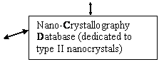
properties, the PI’s group started in the summer of 2005 to develop the
Nano-Crystallography Database (NCD) [21]. The NCD collects data on both the
structure (either complete or to the extent that it is known) and the typical
morphology (tracht and habit) of inorganic nanocrystals in CIF format. Because surface crystallography, the
presence of single or multiple twins, and other nanocrystal specific deviations
form the crystallographic long-range order such as, e.g., core-shell bi-crystal arrangements determine the physical and chemical
properties of nanocrystals, the NCD will
collect and display such information as well. The dependence of the structural prototype, morphology, and structure on
nanocrystal size is also important information that will be collected in the
NCD.
For reference purposes, the
structure and morphology of both larger crystals and type I nanocrystals
(perfect crystals that are simply very small**) will be collected in our
(mainly inorganic) subset of the COD [19] which we will develop further into a
Visual Crystallography Database. The experimental morphological information
that is collected in the “Bestimmungstabellen für Kristalle” [22]
and the “Atlas der Krystallformen” [23] will be the first to be
included in CIF format [20] so that it can later be displayed over the internet
[19].
Because many electron
microscopists and nanocrystal researchers work on rather simple inorganic
structures, we are writing and uploading CIFs to our subset of the COD [19]
(and the COD [18]) in order to support their work. Since our databases are
being developed to support image-based nanocrystallography (i.e. methods that
determine both structure and morphology of nanocrystals from images [2,4,5-10] taken in high resolution TEMs), 3D visualizations
[21] of the entries in these databases are crucial, Fig. 1. (Note that since 1999 the Naval Research
Laboratories have displayed 3D visualizations of the atomic arrangement of
approximately 250 structural prototypes over the internet [24]. Those data are,
however, not available in the versatile CIF format.)
Having more than ten thousand carefully refereed
crystallographic data sets available on the internet in CIF format and under a
sophisticated search engine (that allows, e.g., for Boolean searches on the
basis of cell parameters and the presence or absence of chemical elements in
the crystal) represents a novel resource and allows for many kinds of internet-based
crystallographic calculations and visualizations [21]. This new resource will be for the TEM community and will complement
existing freely accessible internet resources of that community, e.g. refs.
[25-27]. As an example,
we currently provide the ability to calculate lattice-fringe fingerprints in
the dynamical scattering limit from our subset of the COD [19] on our
nanocrystallography web site [28], Fig. 2. In the future, we will also provide
lattice-fringe fingerprint plots in the kinematical scattering limit.
With more than ten thousand critically evaluated
crystallographic data sets already in place at Portland State University [19], we now need to develop effective
computer-based procedures for automated lattice-fringe fingerprint comparisons (search/match
under constraints of known or determined chemical elements present or absent) in order to automate the entire crystal
phase identification procedure, Fig. 3. For processing, the experimental
data that the FEI fingerprinting prototype software delivers will go directly
into newly created software that will derive theoretical expectations (both
kinematic and dynamical limit) for lattice-fringe fingerprint data from freely
accessible CIF-based databases (and store them in derived databases). Next this
newly created software will compare (searches/matches) experimental
lattice-fringe fingerprint data with expectations from theoretical
lattice-fringe fingerprint calculations (under chemical elements present or
absent constraints), and finally will provide a user interface with feedback to
FEI software that supports the recording of high resolution TEM images. For
improved search/matches, lattice-based search/match algorithms on the basis of
CIF data shall be used.
While this software would be of commercial interest to
FEI Company, the derived database of theoretical fringe fingerprint plots (that
has kinematical and a dynamical limit subsets) for the search/match procedures
could be a new product that is of interest to FEI Company, the ICDD, and the
National Institute for Standards and Technology (see letters of support).
Prof. Bryant York, one of the co-PIs of this proposal,
has extensive experience in developing effective search/match algorithms on the
basis of Clifford algebras [29]. As one of the deliverables of the project, the
automated identification of unknown crystal phases will be demonstrated. For
cubic crystals, all interfacial angles between identically indexed net planes
of the conventional cell are the same. In the kinematical limit, space group
information can, therefore, be derived from lattice-fringe fingerprint plots.
It is convenient to normalize the spatial frequency axis and then to compare
the resulting experimental lattice-fringe fingerprint plots with normalized
theoretical lattice-fringe fingerprint plots of all the cubic space groups.
Prof. York’s group will provide algorithms that accomplish this task
effectively.
Many of the available implementations of Fourier
transforms, e.g. Gatan’s Digital Micrograph [30], work only on square or
rectangular areas of images. There are free PC programs, e.g. ImageJ [31], that
calculate Fourier transforms from arbitrarily shaped areas. The image data are,
however, slightly altered in the calculation process since the arbitrarily
chosen area is padded with zeros in order to obtain a square area. In order to
circumvent this data alteration, Prof. York’s group will implement code that
calculates Fourier transforms from arbitrarily shaped images areas without this
padding artefact.
Our collaborators from Shell Chemical LP, Drs. David
Denley and Haskell Hart, are the authors of the Search/Match Databases RINGS
[32] and ZONES [33] that can be employed to identify unknown crystal phases in
a TEM that does not allow for atomic resolution imaging***. The reduced cell
[34] and chemical information of the NIST Crystal Data (Release J. 1997) [35]
constitute the reference data sets for both RINGS and ZONES. Because reduced
cells [34] are unique primitive cells,
they play, together with normalized reduced cells [36], an important role in
identifying unknowns and linking the data on a given crystal phase that appear
in different databases. The normalized reduced cells are especially useful to
identify uncharacterized nanocrystals [36], since their lattice constants may
vary either locally or in the one-percent range over intermediate length scales
depending upon the nanocrystal size. Similarly, the perturbation stable cell
[37] should be applicable for the identification of unknown nanocrystals, since
typical distortions in the angles of reduced unit cells are omitted in
search/match procedure and all metrically similar lattices can be found. We
will, therefore, add the reduced cells, normalized reduced cells, and
perturbation stable cells to the approximately 12,000 CIFs that we currently
make accessible over the internet [19]. In addition, we will, “polish” and
promote Shell Chemical LP’s TEM-based search/match databases along with our new
developments to the wider electron microscopy community. Interestingly, there
are some similarities in the raw data that go into the search/match procedure
for ZONES and those that can be extracted from experimental lattice-fringe
fingerprint plots. We will, therefore, compare the efficiency of the algorithms
that are encoded in ZONES with those we developed.
Having full crystallographic information for more than
ten thousand inorganic crystals (i.e. atomic coordinates, space group,
conventional and reduced unit cell parameters, stoichiometry)
available in CIFs on the internet allows for the simulation of atomic
resolution images and different kinds of electron diffraction patterns directly
on the internet. Source codes for complementary electron microscopic image and
diffraction pattern simulations that are freely available with textbooks such
as e.g. refs. [15], [38] and [39] will be rewritten in follow up projects and
be made available to the electron microscopy community over our
nanocrystallography web site [28].
With support from both our predominantly inorganic
crystal subset of the COD (that we will develop further into an approximately
1500 entry crystal structure and morphology visualization database) and our NCD, lattice fringe fingerprinting
may, in the age of aberration corrected transmission electron microscopy,
become one of the realizations of Boldyrew’s and Doliwo-Dobrowolsky’s 70 years
old prophecy [40]: “In the further
development of crystallography one will either adopt one of the goniometric
methods of determining crystals or develop eventually a new one which, as far
as this is possible, combines the advantages of all of the prior methods and
avoids their disadvantages.”
At the national scale the aberration-correction
revolution in electron optics is spearheaded by Dr. Christian Kisielowski from
the
References
[1] P. Fraundorf, Determining the 3D Lattice parameters of
Nanometer-sized Single
(1987)
[2] P. Moeck, W. Qin, P. Fraundorf, Image-based nanocrystallography
by means of transmission electron goniometry, Nonlinear
Analysis 63, e1323 (2005)
[3] P. Möck, Verfahren zur Durchführung und Auswertung
von elektronenmikroskopischen Untersuchungen, patents DE 4037346 A1
and DD 301839
A7, priority date:
[4]
P. Fraundorf, W. Qin, P.
Moeck, and E. Mandell, Making sense
of nanocrystal lattice fringes, J. Appl. Phys.
98, 114308-1
(2005); arXiv:cond-mat/0212281 v2 (2005)
[5] P. Wang, A.L. Bleloch, U.
Falke, and P.J. Goodhew, Geometric
aspects of lattice contrast visibility in nanocrystalline materials
using HAADF STEM, Ultramicroscopy 106,
277 (2006)
[6] S.J. Pennycook, M.
Varela, C.J.D. Hetherington, and A.I. Kirkland, Materials Advances through Aberration-Corrected Electron
Microscopy, MRS Bulletin 31, 36 (January
2006)
[7] J.R.
Jinschek, H.A. Calderon, K.J. Batenburg, V. Radmilovic, and Ch. Kisielowski,
Discrete Tomography of Ga and InGa
Particles from HREM Image
Simulation and Exit Wave Reconstruction, Mat. Res. Soc. Symp.
Proc. 839, P4.5.1 (2005)
[8] P.
Moeck, O. Čertík, B. Seipel, R. Groebner, L. Noice, G. Upreti,
P. Fraundorf, R. Erni, N. D.
Browning, A. Kiesow, and J.-P.
Jolivet, Identifying uncharacterized nanocrystals by
fringe fingerprinting in two dimensions & free-access crystallographic
databases, Proc.
SPIE Vol. 6000, 60000M-1 (2005)
[9] P. Moeck,
B. Seipel, R. Bjorge, P. Fraundorf, Lattice fringe fingerprinting in two dimensions with database support,
Proc. NSTI
Nanotech
2006,
[10] P. Moeck,
B. Seipel, W. Qin, E. Mandell, and P. Fraundorf, Fringe fingerprinting and transmission electron goniometry,
supporting
image-based nanocrystallography in two and three dimensions, Proc. 9th World
Multi-Congress on Systemics,
Cybernetics
and Informatics, Vol. IX, 249-254,
Materials,
Metrology and Devices”, Session organizer, P. Moeck)
[11] A. Kiesow,
dependent,
periodic line pattern in metal nanoparticle-containing polymer films by femtosecond laser irradiation,
App. Phys. Lett. 86,
153111-1 (2005)
[12] M. Koelsch, S. Cassaignon,
C. Ta Thanh Minh, J.F. Guilemoles, and J.-P.
Jolivet, Electrochemical Comparative
Study of Titania
(Anatase, Brookite and Rutile)
Nanoparticles Synthesized in Aqueous Medium, Thin Solid Films 451/452,
86 (2004)
[13] R.
Könenkamp, P. Hoyer, and A. Wahl, Heterojunctions
and devices of colloidal semiconductor films and quantum dots
J. Appl. Phys. 79, 7029 (2005)
[14] J. Faber,
T. Fawcett, and R. Goehner, The
powder diffraction file (PDF): a relational database
for electron diffraction, Microsc.
Microanal. 11(Suppl.
2), 778 (2005)
[15]
M. De Graef, Introduction
to Conventional Transmission Electron Microscopy,
pp. 55-59
[16] P. Moeck, to be
published
[17] P. Moeck, W. Qin,
and P. Fraundorf, Towards 3D image-based nanocrystallography by means
of transmission electron
goniometry, Mat. Res. Soc.
Symp. Proc. Vol. 839, P4.3.1 (2005)
[18] M. Leslie (Editor), Free the Crystals, Science 310, 597
(2005); D. Chateigner et al., COD (Crystallography Open
Database) and
PCOD (Predicted), Book of Abstracts, XX Congress of the International
Commission on Powder Diffraction, ISSN
1591-9552, http://crystallography.net
[19] http://nanocrystallography.research.pdx.edu/CIF-searchable
[20] S. Hall and B. McMahon
(editors), International Tables for
Crystallography, Vol. G: Definition and exchange of
crystallographic
data, International Union of Crystallography,
[21] P. Moeck, O. Čertík, G. Upreti, B. Seipel,
M. Harvey, W. Garrick, and P. Fraundorf,
dimensions with support from the open access
Nano-Crystallography Database,
J. Mater. Educ. 28(1), 87 (2006)
[22] A.K. Boldyrew and W.W.
Doliwo-Dobrowolsky, Bestimmungstabellen
für Kristalle, (Определитель
Кристаллов),
Vol. I, Part
1 & Part 2, Труды Центрального
научно-исследовательского
Геолого-разведочного Института, Leningrad and Moscow,
1937 and 1939
[23] V.M. Goldschmidt, Atlas der Krystallformen, 1913 –
1923 (9 volumes of crystal drawings and 9 volumes of accompanying text)
[24] http://cst-www.nrl.navy.mil/lattice/index.html
[25] Electron Microscopy Image Simulation -
EMS ON Line, P. Stadelmann, CIME-EPFL; http://cimesg1.epfl.ch/CIOL/
[26] jems, the
[27] Web Electron Microscopy Applications Software
(WebEMAPS), J.M. Zuo and J.C. Mabon,
[28]
http://nanocrystallography.research.pdx.edu
[29] G. Sommer (Ed.), Geometric
Computing with Clifford Algebra, Springer Verlag, 2001
[30] Digital Micrograph, http://www.gatan.com/imaging/dig_micrograph.html
[31] ImageJ, http://rsb.info.nih.gov/ij/
[32] D.R. Denley and H.H. Hart,
RINGS: a search/match database for
identification by polycrystalline electron diffraction, J. Appl.
Cryst. 35, 546 (2002)
[33] H.H. Hart, ZONES: a search/match database for
single-crystal electron diffraction, J. Appl. Cryst. 35, 552 (2002)
[34] A.D. Mighell, Lattice Symmetry and Identification – The
Fundamental Role of Reduced Cells in Materials Characterization, J.
Res. Natl. Inst.
Stand. Technol. 106, 983
(2001)
[35] A.D. Mighell and V.L.
Karen, NIST Crystallographic Databases for Research and Analysis, J. Res. Natl. Inst. Stand. Technol.
101, 273 (1996); available over the
[36] A.D. Mighell, The Normalized Reduced Form and Cell
Mathematical Tools for Lattice Analysis - Symmetry and Similarity, J.
Res. Natl. Inst.
Stand. Technol. 108, 447
(2003)
[37] L.C. Andrews, H.J.
Bernstein and G.A. Pelletier, A Perturbation Stable
Cell Comparison Technique, Acta Cryst.
A36, 248
(1980)
[38] E.J. Kirkland, Advanced
computing in electron microscopy, Plenum,
[39] J.C.H. Spence and J. Zuo, Electron Microdiffraction, Springer,
[40] A.K. Boldyrew and W.W.
Doliwo-Dobrowolsky, Über die
Bestimmungstabellen für Kristalle, Zeits. Krist. A
93, 321 (1936)
Footnotes
* Nanocrystallography has been used
together with the noun electron to describe the development
of parallel-beam nanometer-sized diffraction-based nanocrystallographic
methods; J.M. Zuo, Electron
nanocrystallography, chapter 18 in: Handbook
of Microscopy for Nanotechnology, Eds. N. Yao and Z.L. Wang, Kluwer
Academic Publ., Boston, Dordrecht, New York, London, 2005.
** Nanocrystals and
“crystallographically challenged materials” have been defined as entities and materials with well defined structure
over local and intermediate ranges that can be described rather well by a small
unit cell and a small number of additional parameters. These crystals and
materials lack, however, long-range order because the structural coherence dies
out on a nanometer length-scale. This definition goes beyond perfect crystals
that are simply very small and includes materials where the particle size can
be larger but the structural coherence is only on the nanometer length-scale.
Significant structural distortions that might be considered as classical
defects or nanocrystal specific defects to the average structure may be present
to such an extent that it would make little sense to consider the disorder as a
defect away from the ideal structure. In short, the deviations from the perfect
structure are rather severe in these crystals and materials but remnants of the
crystallinity are apparent. There is at present no comprehensive theoretical
framework for such crystals and materials; S.J.L. Billinge and M.G. Kanatzidis,
Beyond crystallography: the study of disorder,
nanocrystallinity, and crystallographically challenged materials with pair
distribution functions, Chem. Commun. pp. 749 (2004) and P. Juha´s, D.M. Cherba, P.M.
Duxbury, W.F. Punch and S.J.L. Billinge, Ab
initio determination of solid-state nanostructure, Nature 440(30), 655 (2006).
*** Both databases allow for
searches on chemical information (as obtained by, e.g., energy dispersive X-ray
spectroscopy in a TEM) in combination with electron diffraction information in
the dynamical limit (as obtained by selected area electron diffraction in a
TEM). While RINGS tackles polycrystalline electron diffraction data from
unknowns, ZONES is applicable to large (i.e. μm
sized) single crystals.
Appendices
Figures
Rutile Nickel-divanadium Oxide
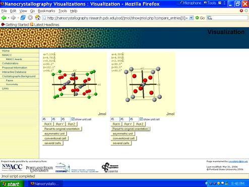
Fig. 1: Screenshot with visualizations in 3D for Nickel-divanadium
Oxide and Rutile.
Rutile
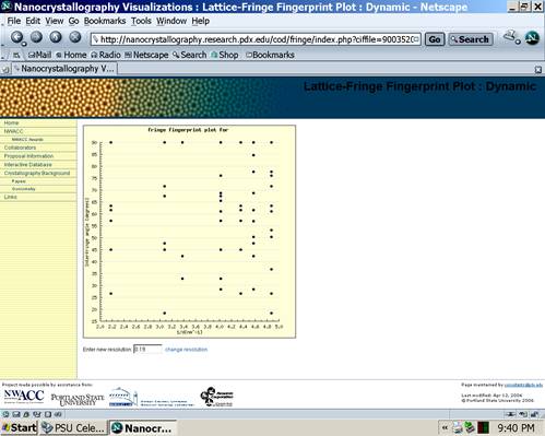
Fig. 2: Screenshot with calculated lattice-fringe
fingerprint for rutile at the dynamical scattering limit.
proposed developments free CIF-based databases
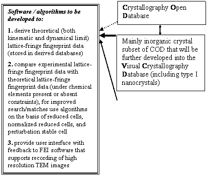
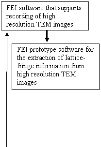

![]()
![]()
Fig. 3: Sketch of the relationships between FEI Company’s software, the
proposed new developments, and the open access CIF-based databases.
Peter Moeck
Assistant
Professor Phone:
503 725 4227
Department of
Physics Fax.: 503
725 9525
![]()
Professional Preparation
Leipzig University Crystallography
M.S. 1983 cum laude (2)
Humboldt University Berlin Crystallography
PhD. 1991 magna cum laude (1)
Appointments
2002 - Tenure-track Assistant Professor
2000 - 2002 Research Assistant Professor
1998 - 2000 Research Fellow (Electron
Microscopist, Materials Scientist)
1997 - 1998 Research Associate (X-ray Crystallographer,
Materials Scientist)
Interdisciplinary Research Centre for
Semiconductor Materials of the Imperial
1994 - 1997 Senior Research Assistant (X-ray Crystallographer,
Materials Scientist)
1993 - 1994 Forensic Scientist / Public Analyst
Central Forensic Science Laboratories of the
German state
1992 - 1993 Electron Microscopist, Computer Programmer, X-ray
Crystallographer
Humboldt-University of
and
1987 - 1991 Scientific Assistant/Staff-PhD (employed primarily to perform research)
Humboldt-University of
Science
1983 - 1986 Crystallographer, Electron Microscopist, Materials
Scientist
Institute for Semiconductor Physics
10 Significant Publications with relevance to this
proposal
• Fraundorf, P.; Qin, W.; Moeck, P.; Mandell, E. "Making sense of
nanocrystal lattice fringes." J.
Appl. Phys. 2005, 98,
114308-1-114308-10,
arxiv.org/abs/cond-mat/0212281, also Virtual Journal of Nanoscale Science and
Technology 2005, Vol. 12, Issue 25, http://scitation.aip.org/dbt/dbt.jsp?KEY
=VIRT01&Volume=12& Issue=25#MAJOR2.
• Moeck P. et al.,
Identifying uncharacterized nanocrystals by fringe fingerprinting in two
dimensions & free-access crystallographic databases, Proc. of SPIE 2005, 6000, 60000M-1-60000M-12.
• Möck, P.; Qin, W.; Fraundorf, Philip B. "Towards 3D image-based
nanocrystallography by means
of transmission
electron goniometry." Materials
Research Society Symposium Proceedings 2005,
839, 93-98.
• Browning, N. D.; Arslan, I.; Ito, Y.; James, E. M.; Klie, R. F.; Möck,
P.; Topuria, T.; Xin, Y.
"Application of atomic scale STEM techniques
to the study of interfaces and defects in materials."
J. Electron Microscopy 2001, 50, 205-218.
• Browning, N. D.; Arslan,
electron
microscopy." Phys. Stat.
Solidi B: Basic Research 2001, 227, 229-245.
• Möck, P. “A Direct Method for Orientation Determination Using TEM (I),
Description of the
Method.” Cryst. Res. Technol. 1991,
26, 653-658
& (II), Experimental Example.” Cryst. Res. Technol. 1991, 26, 797-801.
• Möck P.; Topuria T.; Browning N.D.; Booker G.R.; Mason N.J.; Nicholas
R.J.; Dobrowolska M.; Lee S.; Furdyna J.K. “Internal self-ordering in In(Sb,As), (In,Ga)Sb and (Cd,Mn,Zn)Se
nano-agglomerates/quantum dots”, Appl. Phys. Lett. 2001, 79, 946-948.
• Möck P. “Analysis of thermal treatment induced dislocation bundles in GaAs wafers
by means of X-ray transmission topography and complementary methods”, J. Appl. Cryst. 2001, 34, 65-75.
• Moeck P. ”Quantum dots, semiconductor,
atomic ordering over time”, Dekkler Encyclopaedia of Nanoscience and
Nanotechnology, 2004, 3237-3246
• Moeck P. “Atomic Ordering in Self-Assembled Semiconductor Quantum Dots”, Problems of Nonlinear Analysis in Engineering
Systems 2005, 11,
48-65.
Synergistic Activities
• Member of the International Advisory Board of the Crystallography Open
Database,
www.crystallograpy.net
• Member of the electron diffraction subcommittee of the International
Center for Diffraction Data
• Organizer and session chair of the symposium “Nanotechnology:
materials, metrology, and
devices”
at 9th World Multi-Conference on Systemics, Cybernetics and
Informatics, July 10 – 13,
• Session chair at 11th International Conference on
Composites/Nano Engineering, August 8 - 14,
2004,
Collaborators (past 48 months)
Prof. Nigel D. Browning, Lawrence
Prof. Philip B. Fraundorf,
Dr. Wentao Qin, Technology Solutions, Freescale Semiconductor
Prof. Patrick J. McCann,
Prof. Venkat K. Rao and Dr. Amita Gupta, The
Royal
Prof. Jean-Pierre Jolivet, University
Dr. Andreas Kiesow, Fraunhofer Institute for Materials Mechanics,
Profs.
James E. Morris, Georg Grathoff, Erik Sánches, Chunfei Li, and Dr. Bjoern
Seipel, Portland State University
Graduate, Postdoctoral, and Senior Research
Assistant Advisors
• Prof. Nigel D. Browning,
• Dr. Graham R. Booker, Dept. of Materials, and Prof. Robin J. Nicholas,
Dept. of Physics,
• Profs. Bruce A. Joyce and Paul F. Fewster, Interdisciplinary Research
Centre for Semiconductor
Materials of the Imperial
• Prof. Brian K. Tanner,
• Profs. Dr. Klaus Jacobs Manfred Schenk, Humboldt-University of
Crystallography and Materials
Science
Thesis Advisor and Postgraduate-Scholar Sponsor
supervisor
of 2 postdoctoral researchers, 6 graduate students, 3 undergraduates, 1
American, 2 Swedish and 3 Czech summer students.