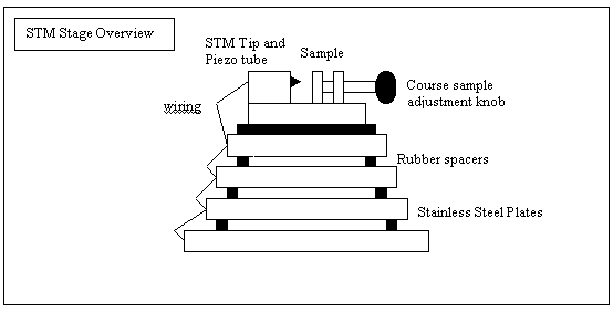
The STM project began Spring term of 1997/98. The STM at this point had not been working since its move to another room in 1996. The intention of this project was to getting the STM working properly again. The Spring term Jeremy spent working on the STM learning worked, how to operate it, and what improvements might be possible.
The main problem turned out to be something rather simple to fix. The STM had been given a faster computer to run the computer software and assorted processing and the software was written for a certain MHz speed computer. Therefore, the faster computer was running the STM operations to fast for the equipment to work properly. This problem was solved temporally by down graded to a slower computer. The STM scans now produced by the slower computer were comparable to previous results before the move.
The next major problem encountered were some electrical connections that were broken. The main tunneling current connection was in very poor shape and this effected the image displayed greatly. Also various little connections were cold soldered or just not connected. Once these connections were fixed things started to run much better and the STM performed with more reliability.
During this time data sheets were accumulated for the components used in the electronics. Jeremy studied how the STM hardware and software were working and looked for potential improvements. This back engineering yielded the necessary information to formulate improvements for the STM system. The following areas of improvement were identified:
The signal being generated by the tunneling current is generally between 0.1nA to 50nA. (Chen, 1993) This means that many sources of noise become significant at these levels. This includes the Pico to nano amperes of current leaking from depletion regions created by connections, leaking capacitors, coupled capacitance and inductance, thermal noise in components, and power line noise. The effects of these noise sources can be diminished if certain precautions and techniques are used.
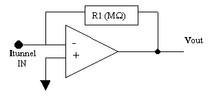
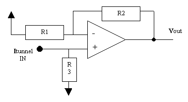
The Portland State University STM uses a shunt amplifier for the pre-amplifier circuit. The picoammeter circuit provides better performance in terms of signal to noise ratio, and amplification bandwidth. This pre-amplifier was designed with these ideas in mind.
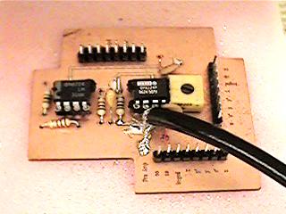
Actual implementation of the new pre-amplifier circuit has not been done due to time constraints. A circuit board and parts has been assembled for the pre-amplifier. Problems with finding compatible connectors for the STM are mainly to blame. Completion of the pre-amplifier circuit requires some additional work.
Changing the voltage reference of the A/D would allow more of the discretized levels to be within the range of the analog input voltage. This in turn would increase the sensitivity of the system and possibly increase the resolution of the acquired data. Therefore, small features could be discernable on the atomic scale of the STM sample.
There is another way to increase the number of discretized levels in the voltage range. This would be to go from a 12bit A/D (4096 levels) to a 16 bit A/D (65536 levels). From this we would acquire more resolution in the data. From a first glance this would seem the choice to make for improving the A/D conversion. One of the problems with the 16 bit A/D is that only so much useful information can be acquired from the STM tip signal.
Another problem with going to a 16 bit A/D is the cost of the circuitry. The average price of a 12 bit A/D with 200KHz sampling rate is around $20. The average price of 16 bit A/D with 200KHz sampling rate is around $50. (*Cost comparisons were done using Digikey Components Supplier catalog). This cost difference can be considered prohibitive when a small resource budget is present.
Some qualitative noise analysis was done on the system. First, the isolation transformer was taken off the circuitry. Therefore, all circuitry was run off the wall power. This created a marked difference in the clarity of the scans. It was not possible to observe atomic resolution while using the wall power. The scans were buried under a layer of noise. Watching the pre-amplifier output showed a signal with very chaotic components and varied amplitudes. When the isolation transformer was then used it was again possible to observe atomic structure in the sample. One alternative to using an expensive isolation transformer is to use batteries to power the STM and pre-amp units. This will eliminated any possibility of noise coming from the power source.
Again the game could be played with the voltage reference. To decrease the voltage reference to 5 volts would decrease the step size to (5 / 4096) 1.22mV or 0.05 nano-meters. To increase the D/A resolution to 16 bits with the 10 volt reference would give a step size of (10 / 65536) 0.152mV or 0.006 nano-meters. This is playing the numbers myth because noise in the system would rapidly limit the resolution of the STM to well above that level. One obvious limiting factor is the one or two atoms that are being used for tunneling. Their dimensions are two orders of magnitude larger than the step size. Also the mechanical vibrations of the tip in the holder would probably be substantially larger than 0.006 nano-meters.
Another tradeoff with increased step size is the needed sampling rate of the A/D to get the data from each D/A step of the tip. Smaller step size would require increases in sampling rate to cover the sample amount of distance by the tip. This requires more expensive A/D chips in addition to D/A chips to produce scans with sufficient speed.
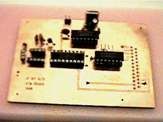
Therefore, with the relative cost and noise issues in mind a 12 bit A/D converter was chosen. A circuit was devised which uses the IBM PC parallel port as I/O for the A/D data. A PIC microcontroller was added to the circuit to control data exchanges and possible do preprocessing of the STM data. The final A/D card has not been integrated into STM due to lack of time, and the need to purchase a PIC microcontroller necessary to complete the circuit. Further development of this circuit can be accomplished with the documentation on the circuit and related STM materials.
Much of the project time was spent trying to get the original A/D and D/A cards working with this new software. Therefore, this left little time to actually finish testing and improving the software. The basic improvements that were incorporated were the following:
1. The user interface is Windows 95 with is GUI capabilities.
2. A timer was used in the code for more precise control over the scanning
and data logging of STM data.
3. The user was able to adjust this rate of scanning to allow for fast
introduction scans or slow more detailed scans.
4. Extraneous undocumented options were out of the program's user front
end.
The actual results of the new STM program were promising since the program was actually producing a scan pattern on the STM and data was being logged to the screen. There were many problems that became evident as initial versions of the program were finished:
1. Visual C++ was much to slow to display the scans in real time. The
program took about 3-4 minutes for one scan, which only produces garbage
from the STM.
2. The slowness of the scanning did not allow the STM to produce atomic
resolution.
3. The actual contrast of the data points was not detectable. Therefore,
the A/D values observed from the scans were so close together that color
associated with them could not be discerned.
Some work was done using a simple digital filtering technique to see if it could improve the values received from the A/D. Since atomic resolution scans were not evident in the pictures generated no real improvement can be determined.
The final version of the program still needs to be developed more to produce satisfactory results on the STM. More work must be done with the contrast of the images. Also new algorithms will have to be developed for faster execution of the screen drawing. It is evident that Microsoft DirectX or WinG resources will need to be used to provide faster direct control of the computer graphics screen.