Scanning Tunneling Microscopy
At
Portland State University

STM Tip:
The ability to resolve atomic features on a sample requires atomic sharpness
on a STM tip. The ideal case is where one atom on the tip is interacting
with the surface (tunneling electrons across the junction). Many articles
describe the manufacturing of STM tips as more of an art than a science.
STM tips expected to be of high quality when micro-graphed by a SEM give
mediocre results, while tips that look like "garbage" when micro-graphed
can give good results while in the STM. There are several procedures available
that increase the production of good tips.
Here are some of the current methods used to obtain atomic resolution
on the tips used in STM's:
1. The simplest method is to use a sharp pair of scissors to cut the
thin Tungsten wire.
2. Chemically Etching is also another method, that is rather easy to
perform but more difficult to get reasonable results. Though this method
does provide much better tips when it works out correctly then using scissors.
3. Purchase tips from a manufacture.
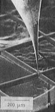
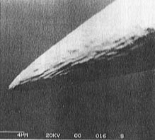
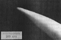
Here are some pictures of the various degrees of atomic tip sharpness: